Multiple Choice
Identify the
choice that best completes the statement or answers the question.
|
|
|
1.
|
In terms of digital logic, a
HIGH voltage usually represents
a. | a zero. | c. | an illegal condition. | b. | an open. | d. | a one. |
|
|
|
2.
|
In term of digital logic, a one
is usually represented by
a. | 0 V. | c. | +10 V. | b. | +5 V. | d. | +15 V. |
|
|
|
3.
|
In terms of digital logic, a
LOW voltage usually represents
a. | an illegal
condition. | c. | a
one. | b. | an open. | d. | a zero. |
|
|
|
4.
|
The Boolean equation for an AND
gate is ________.
a. | A - B =
X | c. | A + B =
X | b. | AB =
X | d. | A/B = X |
|
|
|
5.
|
In order to produce a HIGH
output, an AND gate requires
a. | any input to be
LOW. | c. | all inputs to be
HIGH. | b. | any input to be HIGH. | d. | all inputs to be LOW. |
|
|
|
6.
|
Which logic function is
represented by the equation ABCD = X?
a. | OR | c. | inverter | b. | AND | d. | clock |
|
|
|
7.
|
Which set of outputs is correct
for this AND truth table?
|
|
|
8.
|
The Boolean equation for an OR
gate is ________.
a. | A - B =
X | c. | A/B =
X | b. | A + B =
X | d. | AB = X |
|
|
|
9.
|
In order to produce a LOW
output, an OR gate requires
a. | all inputs to be
HIGH. | c. | any input to be
LOW. | b. | any input to be HIGH. | d. | all inputs to be LOW. |
|
|
|
10.
|
Which set of outputs is correct
for this OR truth table?
|
|
|
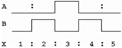
11.
|
Waveforms A and B represent the
inputs to an AND gate. During which time interval will the output from the gate (X) be
HIGH?
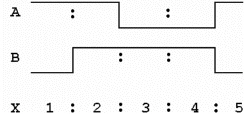
a. | time interval
1 | c. | time interval
4 | b. | time interval
2 | d. | time interval
5 |
|
|
|
12.
|
Waveforms A and B represent the
inputs to an OR gate. During which time intervals will the output from the gate (X) be LOW?
 Wa Wa
a. | time intervals 1 and
2 | c. | time intervals 1 and
4 | b. | time intervals 1 and
3 | d. | It is never
low. |
|
|
|
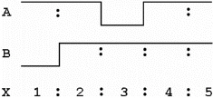
13.
|
Waveforms A and B represent the
inputs to an AND gate. During which time interval will the output from the gate (X) be HIGH?
a. | time interval
1 | c. | time interval
4 | b. | time interval
3 | d. | time interval
5 |
|
|
|
14.
|
If one input of an AND gate is
HIGH while the other is a clock signal, the output is
a. | a clock
signal. | c. | HIGH. | b. | LOW. | d. | cannot be
determined |
|
|
|
15.
|
If one input of an OR gate is
LOW while the other is a clock signal, the output is
a. | LOW. | c. | HIGH. | b. | a clock signal. | d. | cannot be determined |
|
|
|
16.
|
If both inputs of an OR gate
are normally HIGH but one of them momentarily dips LOW, the output will
a. | stay
HIGH. | c. | be
LOW. | b. | go LOW and remain LOW. | d. | momentarily dip LOW. |
|
|
|
17.
|
If one input of an AND gate is
considered to be an enable, it will enable the other input when it is
a. | the same as the other
input. | c. | LOW. | b. | opposite of the other input. | d. | HIGH. |
|
|
|
18.
|
How many two-input gates are in
a single 14-pin DIP integrated circuit?
|
|
|
19.
|
The ground and power pins on a
typical TTL 14-pin DIP are
a. | pins 1 and
14. | c. | pins 7 and
8. | b. | pins 1 and
8. | d. | pins 7 and
14. |
|
|
|
20.
|
Inversion is indicated
by
a. | a bubble on a gate
output. | c. | a triangle on a
gate output. | b. | a bar (line) over a Boolean equation. | d. | all of the above |
|
|
|
21.
|
The Boolean equation for a NAND
function is
a. | X = AB | c. | X =  | b. | X =  | d. | X =   |
|
|
|
22.
|
Which logic gate is described
by the following truth table?
|
|
|
23.
|
Which output is correct for
this NAND truth table?
|
|
|
24.
|
A NOR gate with one HIGH input
and one LOW input
a. | will not
function. | c. | functions as an
AND. | b. | will output a HIGH. | d. | will output a LOW. |
|
|
|
25.
|
Which logic gate is described
by the following truth table?
|
|
|
26.
|
Which logic function can be
implemented by connecting an inverter to the output of an OR gate?
|
|
|
27.
|
If input A of a NAND gate is
connected to a clock and input B is LOW, the normal output is
a. | an inverted clock
signal. | c. | HIGH. | b. | a clock signal. | d. | LOW. |
|
|
|
28.
|
If input A of a NOR gate is LOW
and input B is HIGH, the output should be
a. | unknown. | c. | HIGH. | b. | changing. | d. | LOW. |
|
|
|
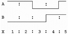
29.
|
Waveforms A and B represent the
inputs to a NAND gate. During which time interval(s) will the output from the gate (X) be
LOW?
a. | time interval
2 | c. | never | b. | time intervals 2, 3, and 4 | d. | time intervals 2 and 3 |
|
|
|
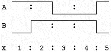
30.
|
Waveforms A and B represent the
inputs to a NOR gate. During which time intervals will the output from the gate (X) be LOW?
a. | all time
intervals | c. | never | b. | time intervals 2, 3, and 4 | d. | time intervals 1 and 5 |
|
|
|
31.
|
What will be the output of a
three-input NOR gate whose inputs are a clock, a HIGH, and a LOW?
a. | clock | c. | HIGH | b. | LOW | d. | cannot be determined |
|
|
|
32.
|
What will be the output of a
three-input NAND gate whose inputs are a HIGH, a HIGH, and a clock?
a. | LOW | c. | a clock signal | b. | HIGH | d. | an inverted clock signal |
|
|
|
33.
|
How many inverters are in a
14-pin DIP integrated circuit?
|
|
|
34.
|
The truth table for a
three-input OR gate contains ________ entries.
|
|
|
35.
|
Assume that a logic gate has
four inputs. How many possible input combinations will be listed in its truth
table?
|
|
|
36.
|
Which logic circuit is
represented by the Boolean equation  = X? = X?
a. | NAND | c. | Clock | b. | AND | d. | Inverter |
|
|
|
37.
|
Which logic circuit is
represented by the Boolean equation  = X? = X?
a. | OR | c. | NOR | b. | Inverter | d. | NAND |
|