Multiple Choice
Identify the
choice that best completes the statement or answers the question.
|
|
|
1.
|
Which statement is true of the
Q and  outputs of any
flip-flop? outputs of any
flip-flop?
a. | Q is a one when the flip-flop is
RESET. | b. | They are always opposite. | c. | They are always opposite when the flip-flop is in the HOLD
condition. | d. | Q is a zero when the flip-flop is
SET. |
|
|
|
2.
|
When a flip-flop is SET,
________.
a. | Q and  =
1 =
1 | c. | Q =
0 | b. |  =
1 =
1 | d. | Q = 1,  =
0 =
0 |
|
|
|
3.
|
When a flip-flop is RESET,
________.
a. | Q = 1,  =
0 =
0 | c. | Q = 0,  =
0 =
0 | b. | Q = 0,  =
1 =
1 | d. | Q =  |
|
|
|
4.
|
The term HOLD means
________.
a. | Q = 0,  =
1 =
1 | c. | Q = 1,  =
0 =
0 | b. | Q = 0,  =
0 =
0 | d. | no change |
|
|
|
5.
|
Which of the following
flip-flops have synchronous inputs?
a. | 7474
D-flip-flop | c. | S-R
flip-flop | b. | NAND flip-flop | d. | all of the above |
|
|
|
6.
|
The logic states of a J-K
flip-flop are SET, RESET, HOLD, and
a. | ENABLE. | c. | TOGGLE. | b. | TRIGGER. | d. | CLEAR. |
|
|
|
7.
|
TOGGLE state of a J-K flip-flop
means that the Q and  outputs will outputs will
a. | switch to Q = 1 and  = 0.
= 0. | c. | switch to
zero. | b. | switch to their opposite state. | d. | become the same as J and K. |
|
|
|
8.
|
If the inputs of a J-K
flip-flop are J = 1 and K = 1 while the outputs are Q = 0 and  = 1, what
will the outputs be after the next clock pulse occurs? = 1, what
will the outputs be after the next clock pulse occurs?
a. | Q = 1,  =
0 =
0 | c. | Q = 1,  =
1 =
1 | b. | Q = 0,  =
0 =
0 | d. | Q = 0,  =
1 =
1 |
|
|
|
9.
|
If the inputs of a J-K
flip-flop are J = 0 and K = 0 while the outputs are Q = 0 and  = 1, what
will the outputs be after the next clock pulse occurs? = 1, what
will the outputs be after the next clock pulse occurs?
a. | Q = 0,  =
1 =
1 | c. | Q = 0,  =
0 =
0 | b. | Q = 1,  =
1 =
1 | d. | Q = 1,  =
0 =
0 |
|
|
|
10.
|
If the inputs of a J-K
flip-flop are J = 1 and K = 0 while the outputs are Q = 0 and  = 1, what
will the outputs be after the next clock pulse occurs? = 1, what
will the outputs be after the next clock pulse occurs?
a. | Q = 0,  =
1 =
1 | c. | Q = 0,  =
0 =
0 | b. | Q = 1,  =
1 =
1 | d. | Q = 1,  =
0 =
0 |
|
|
|
11.
|
If the inputs of a J-K
flip-flop are J = 1 and K = 1, what will the flip-flop do on the next clock
pulse?
a. | TOGGLE | c. | RESET | b. | SET | d. | HOLD |
|
|
|
12.
|
The symbol used on logic
diagrams for an edge-triggered clock input is
a. | a small
circle. | c. | a small
triangle. | b. | a small arrow. | d. |  |
|
|
|
13.
|
A negative edge-triggered
flip-flop will only accept inputs when the clock
a. | is
HIGH. | c. | changes from LOW to
HIGH. | b. | is LOW. | d. | changes from HIGH to LOW. |
|
|
|
14.
|
A positive edge-triggered
flip-flop will only accept inputs when the clock
a. | is
HIGH. | c. | is
LOW. | b. | changes from LOW to HIGH. | d. | changes from HIGH to LOW. |
|
|
|
15.
|
The waveforms below represent
the inputs to a negative edge-triggered J-K flip-flop. At which point(s) will its Q output go
HIGH?
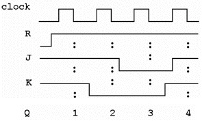
a. | point 1 | c. | point 3 | b. | point 2 | d. | points 3 and 4 |
|
|
|
16.
|
The waveforms below represent
the inputs to a negative edge-triggered J-K flip-flop. At which point(s) will its Q output go
LOW?
a. | point 3 | c. | points 1, 3, and 4 | b. | point 2 | d. | points 1 and 4 |
|
|
|
17.
|
Circuits that operate
sequentially, in step with a control input are called
a. | asynchronous. | c. | synchronous. | b. | memory. | d. | latching. |
|
Matching
|
|
|
|
|
|
18.
|
Active Low Input
|
|
|
19.
|
Active High Input
|
|
|
20.
|
Negative Edge Trigger
|
|
|
21.
|
Positive Edge Trigger
|
Problem
|
|
|
22.
|
For the 74LS74 D flip-flop shown below, complete the
timing diagram for the output signal Que. Note that the CLK input for this flip-flop is
a positive edge trigger and both the PR and CLR asynchronous inputs are active
low.
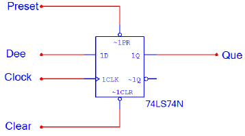
Draw out the following timing diagram
and then complete what the output Que (Shown started in red) will look like. Show me your
completed timing diagram. In your answer below write “shown in
class”
Que | | | | | | | | | | | | | | | | | | | | | | | | | | | | | | | | | | | | | | | | | | | | | | | | | | | | | Dee | | | | | | | | | | | | | | | | | | | | | | | | | | | | | | | | | | | | | | | | | | | | | | | | | | | | | Preset | | | | | | | | | | | | | | | | | | | | | | | | | | | | | | | | | | | | | | | | | | | | | | | | | | | | | Clear | | | | | | | | | | | | | | | | | | | | | | | | | | | | | | | | | | | | | | | | | | | | | | | | | | | | | Clock | | | | | | | | | | | | | | | | | | | | | | | | | | | | | | | | | | | | | | | | | | | | | | | | | | | |
|
|
|
23.
|
For the 74LS76 J/K flip-flop shown below, complete the
timing diagram for the output signal Que. Note that the CLK input for this flip-flop is
a negative edge trigger and both the PR and CLR asynchronous inputs are active
low.
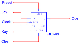
Draw out the
following timing diagram and then complete what the output Que (Shown started in red) will look
like. Show me your completed timing diagram. In your answer below write “shown in
class”
Que | | | | | | | | | | | | | | | | | | | | | | | | | | | | | | | | | | | | | | | | | | | | | | | | | | | | | Jay | | | | | | | | | | | | | | | | | | | | | | | | | | | | | | | | | | | | | | | | | | | | | | | | | | | | | Kay | | | | | | | | | | | | | | | | | | | | | | | | | | | | | | | | | | | | | | | | | | | | | | | | | | | | | Preset | | | | | | | | | | | | | | | | | | | | | | | | | | | | | | | | | | | | | | | | | | | | | | | | | | | | | Clear | | | | | | | | | | | | | | | | | | | | | | | | | | | | | | | | | | | | | | | | | | | | | | | | | | | | | Clock | | | | | | | | | | | | | | | | | | | | | | | | | | | | | | | | | | | | | | | | | | | | | | | | | | | |
|
|
|
24.
|
When flip-flops were discussed briefly back in unit (1),
we saw that a D flip-flop could be used to create a Divide-By-Two circuit. Remember, a
Divide-By-Two circuit is one that generates a clock output that is half the frequency of the
clock input. Likewise, a Divide-By-Two circuit can be implemented with a J/K flip-flop. See
below.
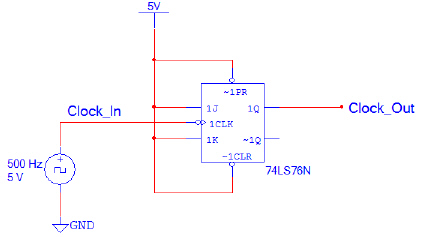
J/K
Divide-By-Two Circuit
a. Complete the timing
diagram shown below for a J/K Divide-By-Two circuit. Show me your timing
diagram.
b. Using the Multisim, enter the
Divide-By-Two circuit. Add an
oscilloscope to monitor the two signals Clock_In and Clock_Out. Run the simulation and
capture several periods of the output signal. Verify that the circuit is working as expected and that
the output signal matches the predictions from step (a). If the results do not match, review your
work and make any necessary corrections. Show me your completed circuit simulating in
Multisim.
c. Change the frequency of Clock_In to 20 KHz
and re-simulate. What effect did this change have on the frequency of the output signal
Clock_Out?
Make sure that you write “checked off in class for your
answer”
|
|
|
25.
|
The circuit shown below generates two
non-overlapping signals at the same frequency. These signals, C-OUT1 and C-OUT2, were
frequently used by early microprocessor systems that required four different clock transitions all
synchronized by one clock.
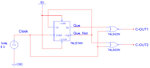
Non-Overlapping Signal Generator
a. Complete the timing
diagram shown below for the Non-Overlapping Signal Generator circuit. Show me your completed
timing diagram.
C-OUT2 | | | | | | | | | | | | | | | | | | | | | | | | | | | | | | | | | | | | | | | | | | | | | | | | | | | | | | | | | | | C-OUT1 | | | | | | | | | | | | | | | | | | | | | | | | | | | | | | | | | | | | | | | | | | | | | | | | | | | | | | | | | | | Que_Not | | | | | | | | | | | | | | | | | | | | | | | | | | | | | | | | | | | | | | | | | | | | | | | | | | | | | | | | | | | Que | | | | | | | | | | | | | | | | | | | | | | | | | | | | | | | | | | | | | | | | | | | | | | | | | | | | | | | | | | | Clock | | | | | | | | | | | | | | | | | | | | | | | | | | | | | | | | | | | | | | | | | | | | | | | | | | | | | | | | | |
b. Using the CDS, enter the
Non-Overlapping Signal
Generator circuit. Add an oscilloscope to monitor the three signals Clock, C-OUT1,
and C-OUT2. Run the simulation and capture several periods of the output signals. Verify that
the circuit is working as expected and the output signals match the predictions from step (a). If the
results do not match, review your work and make any necessary correction. Show me your completed
circuit on multisim.
c. The input signal, Clock, was a 1 KHz
square wave with a 50% duty cycle. What is the frequency and duty cycle of the output signals
C-OUT1 and C-OUT2? Remember Frequency is 1/period and that duty cycle is
time_high/Period X 100. Write these in for your answers.
d.
Change the frequency of Clock to a 2 KHz and re-simulate. What effect did this change have on
the frequency of the output signals C-OUT1 and C-OUT2?
|