Multiple Choice
Identify the
choice that best completes the statement or answers the question.
|
|
|
1.
|
The Boolean equation for the
exclusive-OR function is
|
|
|
2.
|
When the inputs to an
exclusive-OR gate are the same logic level, the output is
a. | zero. | c. | one. | b. | HIGH. | d. | cannot tell |
|
|
|
3.
|
During which time interval(s)
will output X of this XOR timing diagram be LOW?
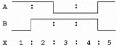
a. | time interval
1 | c. | time intervals 3 and
4 | b. | time interval
2 | d. | time intervals 4 and
5 |
|
|
|
4.
|
During which time interval(s)
will output X of this XOR timing diagram be HIGH?
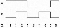
a. | time intervals 1, 3, and
5 | c. | time intervals 2 and
4 | b. | time intervals 1, 4, and
5 | d. | time interval
3 |
|
|
|
5.
|
What is the correct set of
output values for this XOR truth table?
A
B X
0 0
0 1
1
0
1 1
a. | X =
0
1
1
1 | b. | X = 0
0
0
1 | c. | X =
0
1
1
0 | d. | X = 0
0
1
1 |
|
|
|
6.
|
The Boolean equation for the
exclusive-NOR function is
a. | X = A + B +  +
+  . . | c. | X = AB +   . . | b. | X =  . . | d. | X = AB +  . . |
|
|
|
7.
|
When the inputs to an
exclusive-NOR gate are unequal, the output is
a. | one. | c. | zero. | b. | HIGH. | d. | cannot tell |
|
|
|
8.
|
During which time interval(s)
will output X of this XNOR timing diagram be LOW?
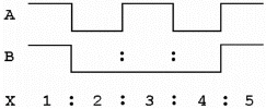
a. | time intervals 1, 2, 4,
5 | c. | time interval
1 | b. | time intervals 1 and
5 | d. | time interval
3 |
|
|
|
9.
|
During which time interval(s)
will output X of this XNOR timing diagram be HIGH?
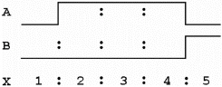
a. | time interval
1 | c. | time interval
5 | b. | time intervals 2, 3, and
4 | d. | time intervals 1 and
5 |
|
|
|
10.
|
What is the correct output for
this XNOR truth table?
A
B X
0 0
0
1
1
0
1 1
a. | X =
1
1
1
0 | b. | X = 0
1
1
0 | c. | X =
1
0
0
1 | d. | X = 0
1
1
1 |
|
|
|
11.
|
A HIGH output if one or the
other inputs is HIGH, but not both; describes a(n) ________ gate.
|
|
|
12.
|
If the same signal is connected
to both inputs of an XOR gate, the output is
a. | undetermined. | c. | HIGH. | b. | LOW. | d. | a clock
waveform. |
|
|
|
13.
|
Use your two bit adder to do the following binary addition.
0101
+ 0111
|
|
|
14.
|
Use your two bit adder to do the following binary addition.
0011
+ 1001
|
|
|
15.
|
Use your two bit adder to do the following binary addition.
1001
+ 0101
|
|
|
16.
|
Use your two bit adder to do the following binary addition.
1010
+ 1101
|
|
|
17.
|
This is an ___________ logic gate. 
|
|
|
18.
|
This is an ___________ logic gate. 
|
Problem
|
|
|
19.
|
Using the Multisim, enter the 2-bit adder shown
below. This adder is implemented with SSI logic (i.e., AND gates, OR gates, and XOR gates).
This circuit has two 2-bit inputs (X1, X0 and Y1, Y0) and three outputs (S2, S1, and
S0). S2-S0 is the sum of adding together X1-X0 and Y1-Y0. Additionally, the outputs (S2-S0) are
connected to a common anode seven-segment display through a 74LS47 display driver.
Note: The wires
are color coded to help with readability; these colors do not need to be maintained in your
drawing.
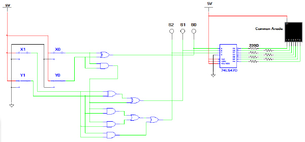
Verify that the circuit is working as expected by completing the truth table
shown.
Inputs | Outputs | X1 | X0 | X | Y1 | Y0 | Y | S2 | S1 | S0 | Display | 0 | 0 | 0 | 0 | 0 | 0 | | | | | 0 | 0 | 0 | 0 | 1 | 1 | | | | | 0 | 0 | 0 | 1 | 0 | 2 | | | | | 0 | 0 | 0 | 1 | 1 | 3 | | | | | 0 | 1 | 1 | 0 | 0 | 0 | | | | | 0 | 1 | 1 | 0 | 1 | 1 | | | | | 0 | 1 | 1 | 1 | 0 | 2 | | | | | 0 | 1 | 1 | 1 | 1 | 3 | | | | | 1 | 0 | 2 | 0 | 0 | 0 | | | | | 1 | 0 | 2 | 0 | 1 | 1 | | | | | 1 | 0 | 2 | 1 | 0 | 2 | | | | | 1 | 0 | 2 | 1 | 1 | 3 | | | | | 1 | 1 | 3 | 0 | 0 | 0 | | | | | 1 | 1 | 3 | 0 | 1 | 1 | | | | | 1 | 1 | 3 | 1 | 0 | 2 | | | | | 1 | 1 | 3 | 1 | 1 | 3 | | | | | | | | | | | | | | |
Make sure that you show me your circuit and completed truth table in
class. We may breadboard this circuit. Fill in the answer to this problem with completed in
class.
|
|
|
20.
|
Use the Multisim to enter the 2-bit adder shown
below. This adder is implemented with 74LS183 MSI full add gates.
This circuit is
functionally identical to the SSI implementation from step number 1.
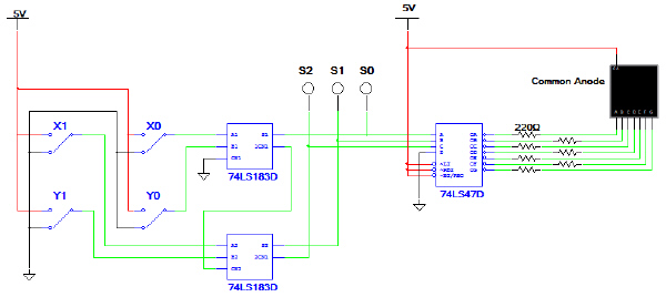
Verify that the circuit
is working as expected by completing the truth table shown.
Inputs | Outputs | X1 | X0 | X | Y1 | Y0 | Y | S2 | S1 | S0 | Display | 0 | 0 | 0 | 0 | 0 | 0 | | | | | 0 | 0 | 0 | 0 | 1 | 1 | | | | | 0 | 0 | 0 | 1 | 0 | 2 | | | | | 0 | 0 | 0 | 1 | 1 | 3 | | | | | 0 | 1 | 1 | 0 | 0 | 0 | | | | | 0 | 1 | 1 | 0 | 1 | 1 | | | | | 0 | 1 | 1 | 1 | 0 | 2 | | | | | 0 | 1 | 1 | 1 | 1 | 3 | | | | | 1 | 0 | 2 | 0 | 0 | 0 | | | | | 1 | 0 | 2 | 0 | 1 | 1 | | | | | 1 | 0 | 2 | 1 | 0 | 2 | | | | | 1 | 0 | 2 | 1 | 1 | 3 | | | | | 1 | 1 | 3 | 0 | 0 | 0 | | | | | 1 | 1 | 3 | 0 | 1 | 1 | | | | | 1 | 1 | 3 | 1 | 0 | 2 | | | | | 1 | 1 | 3 | 1 | 1 | 3 | | | | | | | | | | | | | | |
Make sure that
you show me your circuit and completed truth table in class. We may breadboard this circuit.
Fill in the answer to this problem with completed in class.
|