Multiple Choice
Identify the
choice that best completes the statement or answers the question.
|
|
|
1.
|
In terms of digital logic, a
HIGH voltage usually represents
a. | a zero. | c. | an illegal condition. | b. | an open. | d. | a one. |
|
|
|
2.
|
In term of digital logic, a one
is usually represented by
a. | 0 V. | c. | +10 V. | b. | +5 V. | d. | +15 V. |
|
|
|
3.
|
In terms of digital logic, a
LOW voltage usually represents
a. | an illegal
condition. | c. | a
one. | b. | an open. | d. | a zero. |
|
|
|
4.
|
In terms of digital logic, a
zero is usually represented by
a. | -5 V. | c. | +2 V. | b. | 0 V. | d. | -10 V. |
|
|
|
5.
|
In order to produce a HIGH
output, an AND gate requires
a. | any input to be
LOW. | c. | all inputs to be
HIGH. | b. | any input to be HIGH. | d. | all inputs to be LOW. |
|
|
|
6.
|
Which logic function is
represented by the equation AB = X?
|
|
|
7.
|
Which logic function is
represented by the equation ABCD = X?
a. | OR | c. | inverter | b. | AND | d. | clock |
|
|
|
8.
|
The Boolean equation for an AND
gate is ________.
a. | A - B =
X | c. | A + B =
X | b. | AB =
X | d. | A/B = X |
|
|
|
9.
|
The Boolean equation for an OR
gate is ________.
a. | A - B =
X | c. | A/B =
X | b. | A + B =
X | d. | AB = X |
|
|
|
10.
|
In order to produce a LOW
output, an OR gate requires
a. | all inputs to be
HIGH. | c. | any input to be
LOW. | b. | any input to be HIGH. | d. | all inputs to be LOW. |
|
|
|
11.
|
Which logic function is
represented by the equation A + B = X?
|
|
|
12.
|
If one input of an OR gate is
HIGH while the other is a clock signal, the output is
a. | LOW. | c. | a clock signal. | b. | HIGH. | d. | cannot be determined |
|
|
|
13.
|
If one input of an AND gate is
HIGH while the other is a clock signal, the output is
a. | a clock
signal. | c. | HIGH. | b. | LOW. | d. | cannot be
determined |
|
|
|
14.
|
If both inputs of an AND gate
are normally HIGH but one of them momentarily dips LOW, the output will
a. | momentarily dip
LOW. | c. | stay
HIGH. | b. | be LOW. | d. | go LOW and remain LOW. |
|
|
|
15.
|
If both inputs of an OR gate
are normally HIGH but one of them momentarily dips LOW, the output will
a. | stay
HIGH. | c. | be
LOW. | b. | go LOW and remain LOW. | d. | momentarily dip LOW. |
|
|
|
16.
|
How many two-input gates are in
a single 14-pin DIP integrated circuit?
|
Multiple Response
Identify one
or more choices that best complete the statement or answer the question.
|
|
|
17.
|
Using Multisim, enter the Inverter Gate test
circuit shown below. Use a switch for the input X and a probe for the output Z. Toggle the switch to
complete the truth table shown.
Note: When the switch is at GND, the input is a (0).
When it is at +5V, the input is a (1). Likewise, when the probe is on, the output is a (1).
When the probe is off, the output is a (0). SHOW ME YOUR WORKING CIRCUIT.
Select all the answers that are true for this truth table
shown above.
|
|
|
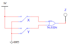
18.
|
Using Multisim, enter the AND Gate test circuit shown
below. Use switches for the inputs X & Y and a probe for the output
Z. Toggle the switches to complete the truth table shown.
Simulating your circuit on Multisim, select ALL of the answers
below that are true for the following truth table. a. | X=0, Y=0, Z= 0 | e. | X=1, Y=0, Z= 0 | b. | X=0, Y=0, Z= 1 | f. | X=1, Y=0, Z= 1 | c. | X=0, Y=1, Z= 0 | g. | X=1, Y=1, Z= 0 | d. | X=0, Y=1, Z=
1 | h. | X=1, Y=1, Z= 1 |
|
|
|
19.
|
Using Multisim, enter the OR Gate test circuit shown
below. Use switches for the inputs X & Y and a probe for the output
Z. Toggle the switches to complete the truth table shown.
Simulating your circuit on Multisim, select ALL of the answers
below that are true for the following truth table. a. | X=0, Y=0, Z= 0 | e. | X=1, Y=0, Z= 0 | b. | X=0, Y=0, Z= 1 | f. | X=1, Y=0, Z= 1 | c. | X=0, Y=1, Z= 0 | g. | X=1, Y=1, Z= 0 | d. | X=0, Y=1, Z=
1 | h. | X=1, Y=1, Z= 1 |
|
Problem
|
|
|
20.
|
Now it’s time for you
to implement your first AOI combinational logic circuit. The circuit that we will use for this
purpose is the Car Safety Buzzer design that was first introduced in the presentation associated with
this activity. The design specifications for this design are as follows: The Buzzer is On whenever
the Door is Open OR when the Key is in the ignition AND the seat belt is NOT
buckled.
Using Multisim, enter the Car Buzzer circuit
shown below. Use switches for the inputs Seatbelt, Key & Door and a probe for the output
Buzzer.
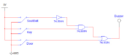
Toggle the input switches to complete the Actual
Buzzer Output column in the truth table shown below.
Inputs | Buzzer
Output | SeatBelt | Key | Door | Actual | Expected | 0 | 0 | 0 | | 0 | 0 | 0 | 1 | | 1 | 0 | 1 | 0 | | 1 | 0 | 1 | 1 | | 1 | 1 | 0 | 0 | | 0 | 1 | 0 | 1 | | 1 | 1 | 1 | 0 | | 0 | 1 | 1 | 1 | | 1 | | | | | |
If the Actual Buzzer Output
column matches the Expected Output column, then your first combinational logic circuit works.
Email me a pdf of your circuit and
completed truth table. If the Actual Output does not match the Expected Output, review your
circuit diagram and make any necessary correction and retest.
Next step, breadboard this
circuit.
|